My headphone amplifier
This page is my design of a headphone amplifier. It’s something I’ve wanted to attempt since I was at uni and never got around to doing it.
Design Goals
- Class-A output.
- Possibility of high (greater than 15 V) output supply voltages.
- Current-mode output.
No use of op-amps.- Completely my own design (no looking at other work on the interwebs to “help” me figure this out).
The first two goals were simply because that seems to be what people like to hear. Whether they actually “hear” it in the output or whether it’s just some marketing snob-factor gimmick, I don’t really care. It made the design a bit more challenging which was what I wanted.
Current-mode output is what really distinguishes this amplifier from other designs (I think?). Considering that a speaker is just a glorified electro-magnet (I was hoping for that to be humorous - please don’t take it seriously) and that magnetic field strength is related to current, i.e. not necessarily Voltage, I wanted to see what would happen if the output of my amplifier was current. So whereas most amplifiers seem to be Voltage-in/Voltage-out devices, this thing is a Voltage-in/current-out (transconductance amplifier) design. Wild.
I had a requirement early on that I would not use op-amps at all in the design, but I eventually scrapped that requirement for the following reasons:
- They make the design so much simpler.
- I can still use them with a high supply voltage in this design as the op-amp supply is separate to the main output supply.
- Did I mention they make the design SO much simpler?
If you’re a non-op-amp purist - this design will not be your thing.
The final point was really the most important criteria for my design - I wanted this design to be completely original. I didn’t want any other designs out there to influence how I put this together. I didn’t want wise-experienced people to tell me exactly what to do. I wanted to get it wrong over-and-over until I got something that worked. I haven’t done this before and wanted a challenge.
Overall description of the circuit
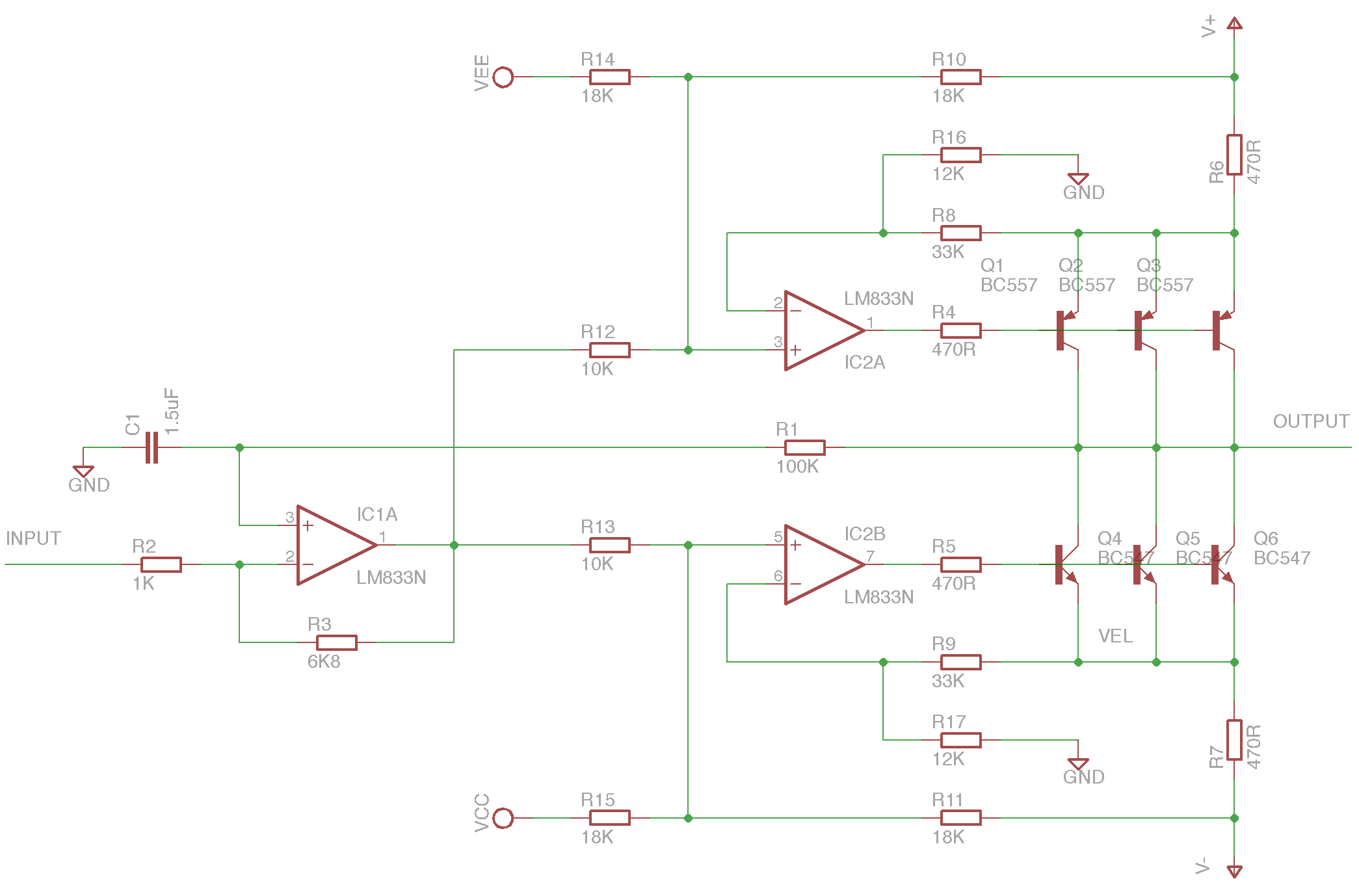
- \(IC_{1a}\) serves two purposes: inversion and buffering of the input and a servo to get rid of any DC present at the output. THIS IS REALLY IMPORTANT IF THE SPEAKER IS CAPACITIVELY COUPLED TO THE OUTPUT! I used \(IC_{1b}\) for the same purpose on the second channel.
- \(IC_2\) drives the upper and lower output transistors.
- \(R_{10}\) and \(R_{11}\) are used to cancel out noise which might be riding on the main output power supply and are critical components when the output stage supply is not regulated.
- \(R_6\) and \(R_7\) are used to sense the emitter current of the drive transistors and also reduce the effect of the transistors DC gain.
- \(R_{14}\) and \(R_{15}\) are used to set the quiescent current and are connected to the same power supply as the op-amps. This supply must be regulated but does not need to supply much current.
- \(R_1\) and \(C_1\) configure the low-pass filtering characteristic of the DC removal servo. The values suggested in the schematic give a time constant of 0.15 seconds. Larger capacitor values can be used but they affect the settling time of the amplifier. Smaller capacitor values WILL NEGATIVELY IMPACT the bass reproduction of this amplifier.
- \(R_8\), \(R_9\), \(R_{16}\) and \(R_{17}\) reduce the emitter voltages to something that the op-amp can work with. The also configure current gain.
- \(R_2\) and \(R3\) are for configuring gain at the input stage.
- The output uses three transistors connected in parallel - call me an idiot, I don’t care, it means I can dissipate more current and use signal rather than power transistors. Use less at your own peril. Or move to a power transistor output and risk the DC current gain (which is always very variable in transistors) corrupting the design parameters.
The maths…
This circuit is simple to analyse (thank you op-amps) and then even simpler because it is symmetric. I’m going to ignore \(IC_1\) and the servo as it what they do can be understood from inspection (they were also the very last things I added to the circuit to correct the output polarity and obliterate leakage currents). I’ll start from the output of \(IC_1\) denoting it as \(V_y\) and I’ll walk through the negative current (low part) of the design.
Let the non-inverting input of \(IC_{2B}\) be denoted as \(V_x\):
\[ V_x = \frac{ R_{15} R_{11} V_{y} + V_{cc} R_{11} R_{13} + V_{-} R_{13} R_{15} }{ R_{15} R_{11} + R_{11} R_{13} + R_{13} R_{15} } \]
Provided that \(IC_{2B}\) is set up correctly in a negative feedback configuration (which we will assume it is based on the values of \(R_{9}\) and \(R_{17}\)), the inverting voltage will also equal \(V_x\) meaning that the current through \(R_{17}\) will equal \(\frac{V_x}{R_{17}}\) and the voltage at the emitters (denoted as \(V_{el}\)) will equal:
\[ V_{el} = V_x \frac{R_{17} + R_9}{R_{17}} \]
Meaning that the emitter current \(I_{el}\) is:
\[ I_{el} = \frac{V_{el} - V_{-}}{R_7} + \frac{V_x}{R_{17}} = \frac{V_x (R_7 + R_9 + R_{17} ) - V_{-} R_{17} }{ R_7 R_{17} } \]
This is where the network of \(R_{11}\), \(R_{13}\) and \(R_{15}\) becomes pretty important. If we substitute in the expression for \(V_x\), into the above, note that we can choose values for these components that will (within component tolerances) cancel out the \(V_{-}\) term which will remove power supply noise from the output. This is absolutely critical if the output power stages of the amplifier is going to run off an unregulated supply. On my prototype I am running it on an unregulated supply and for the left channel (where I had 1% resistors throughout) there was no audible hum. On the other channel I did however have a very mild hum. The other solution here is to run two regulated supplies, but it is still a good thing to try and cancel any noise possible.
After substituting the expression for \(V_x\) into the above, you can find the contributions which \(V_y\), \(V_{-}\) and \(V_{cc}\) make to the emitter current.
\(I_{clV_{-}}\) is the contribution from the output power supply. We want to set this to zero as part of our design:
\[ I_{clV_{-}} = V_{-} \frac{\beta}{\beta + 1} \frac{R_{13} R_{15} (R_7 + R_9 + R_{17}) - ( R_{15} R_{11} + R_{11} R_{13} + R_{13} R_{15} ) R_{17} }{R_7 R_{17} ( R_{15} R_{11} + R_{11} R_{13} + R_{13} R_{15} ) } \]
\(I_{clV_{cc}}\) is the contribution from our stable regulated power supply. This configures the quiescent current draw:
\[ I_{clV_{cc}} = V_{cc} \frac{\beta}{\beta + 1} \frac{R_{11} R_{13} (R_7 + R_9 + R_{17})}{R_7 R_{17} ( R_{15} R_{11} + R_{11} R_{13} + R_{13} R_{15} )} \]
\(I_{clV_y}\) is the contribution from the input section and determines our voltage/current gain:
\[ I_{clV_y} = V_y \frac{\beta}{\beta + 1} \frac{R_{11} R_{15} (R_7 + R_9 + R_{17})}{R_7 R_{17} ( R_{15} R_{11} + R_{11} R_{13} + R_{13} R_{15} )} \]
Design process and component selection
- Set \(R_7\) and \(R_{11}\) using your experience. \(R_7\) greatly impacts output current capabilities. \(R_{11}\) will provide a ball-park range for \(R_{13}\) and \(R_{15}\).
- Your regulated op-amp rails \(V_{cc}\) and \(V_{ee}\). These should be equal and oposite - I used +/- 13.5 Volts because I am nuts. I don’t really like driving op-amps at their maximum ratings.
- Guesstimate your output supply \(V_{+}\) and \(V_{-}\). Mine was +/- 20 Volts because that was what my AC plug-pack happened to give me.
- Guesstimate the current gain (\(\beta\)) of your output transistors. I used 300 for my BC547/557 transistors but it won’t influence the design too much unless it starts getting small (less than 100).
- Pick a quiescent current \(I_q\). My design uses 28.5 mA. If your output current exceeds this value, your amplifier will enter class AB mode.
- Pick a Voltage/current gain \(A\) for the amplifier. My design uses 3.81 mA/V. Note that this will be the current gain for \(V_y\) which is not the input voltage and we are only designing for one HALF of the design (remember, we are relying on symmetry). i.e. the total gain is actually this gain multiplied by the gain configured using \(IC_1\) multiplied by two.
- Define a value \(K\). This value is arbitrary and does not influence the design parameters. It is used as a scale factor for two of the resistors which is useful to get them to match up with E-12 values. The value I ended up using was 15096.
Derive the other components from these values.
\[ R_{15} = \frac{ R_{11} \beta V_{cc} }{ I_q (\beta + 1) R_7 } \]
\[ R_{13} = \frac{ R_{11} \beta }{ A (\beta + 1) R_7 } \]
\[ R_{17} = \frac{ R_{13} R_{15} }{ K } \]
\[ R_9 = \frac{ R_{15} R_{11} + R_{11} R_{13} + R_{13} R_{15} }{ K } - R_7 - R_{17} \]
Once you’ve done this, derive the value for \(V_{el}\) at the quiescent current (i.e \(V_{y} = 0\) )- you want this value floating somewhere around \(\frac{V_{ee}}{2}\). The closer it is to this value, the better. If it is much less than this value, your design is broken as the op-amp will not be able to supply the drive voltage. Just in writing this, I’ve realised that I probably could have made things a bit better by adding a resistor from the base of the transistor bases to \(V_{-}\) to enable larger output voltage swings… design fail. Maybe I’ll revisit this another day.
Note that in this design: \[ R_{2x} = R_{2x+1} \text{ for } x \geq 2 \]
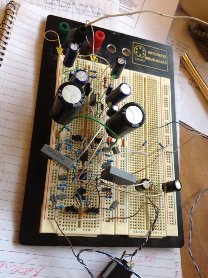
I’ve not included the power supply on this page… I could draw it up if somebody really wanted it - but it’s not complicated. I used an LM317 and LM337 to get my regulated rails which were themselves sourced via a 15 Ohm and 1 mF RC network from the the main +/- 20 Volt supply. My output supply was just the unregulated output from my plug pack with about 5 mF of capacitance for each rail. Copy my breadboard layout. :)
Things to be aware of:
- You may want to use higher quiescent currents than what I used in your design to stay in class A for longer. Particularly if you are driving low resistance headphones. This means that \(R_6\) and \(R_7\) will need to be lowered and you will need to be careful about power dissipation in these components and the drive transistors.
- You may want to either parallel-up a few resistors for \(R_6\) and \(R_7\) or use a 1+ Watt resistor. Most of the output current is dissipated in here. I use 1/4 Watt resistors on my breadboard - but that’s just because I didn’t exactly have a lot of space. They get warm but I don’t care.
- When designing, if your quiescent current is too low, the output will become class AB at high output levels… not a massive issue - just be aware.
- Grounding is massively important. Getting this thing to actually work on a breadboard with the power supply on the same board was quite difficult. The green wire half-way along the board is connecting the two ground lines. This link is made in two other locations on the breadboard but without this one, there is hum. I don’t expect this will be even slightly a problem if (when?) I get this built onto a PCB and do a proper layout.
- As mentioned at the beginning of this post in all-caps: the DC servo component of this design is very important especially if there is a capacitor coupling the headphones to the output. Because actually outputs current, if the bias is not cancelled, the voltage across a coupling capacitor will gradually increase/decrease over time until it reaches a voltage which the amplifier cannot supply anymore causing the output to start crackling and sound terrible (after many seconds of playback). It could also pose a very serious problem to the coupling capacitor if it is polarised or does not have a high-Voltage rating. This problem can be solved somewhat by placing a resistor from the output to ground which will restrict the maximum Voltage that can build-up across the capacitor. But the servo is a much nicer solution and also ensures that there is no pop when headphones are plugged in or out while the unit is powered on. Do it.
- Don’t power the unit on with headphones connected - it really does not sound nice and could break something.
- You could use the same power supply for the output as for the op-amps as long as it is very cleanly regulated.
How does it sound?
I think it sounds great - good enough that I’ll probably get a PCB drawn up and made so that I can have one at work (if I do, I’ll attach it to this page). The design has particularly good (and epically fast) bass reproduction on my HD555 headphones. At the end of the day, you build it and decide for yourself if you like it or not.
If you do build this, please let me know what you think of it (good, bad, what sucks, what’s cool). Also, if you do electrical design, please criticise my design.